Table of Contents
What is Monocrystalline Silicon Annealing?
Monocrystalline silicon annealing is a heat treatment process in which the material is heated to a specific temperature, held in a controlled environment for a certain duration, and then slowly cooled.
The primary purpose of annealing is to improve the crystal quality of monocrystalline silicon, relieve internal stress, repair defects, and optimize its physical and electronic properties, thereby meeting the application requirements in the semiconductor and photovoltaic fields.
Purposes of Annealing
Relieving Internal Stress:
During the growth, slicing, and processing of monocrystalline silicon, internal stresses may develop, leading to crystal deformation or defects. Annealing rearranges atoms through heating, relieving stress and restoring crystal integrity.
Repairing Crystal Defects:
Crystal defects such as dislocations, micro-cracks, and vacancies can occur during the growth process of monocrystalline silicon. Annealing promotes the diffusion of silicon atoms, reducing or eliminating these defects and enhancing structural integrity.
Increasing Carrier Lifetime:
Annealing reduces impurity concentrations and defect densities in silicon, lowering the recombination probability of carriers during migration and thereby improving carrier lifetime.
Regulating Dopant Distribution:
In semiconductor device fabrication, annealing enables dopant atoms to redistribute within the silicon crystal, forming a uniform doping concentration to meet device performance requirements.
Improving Surface and Interface Quality:
Annealing helps reduce oxide layers and other contaminants on the surface of monocrystalline silicon, improving surface flatness and interface quality, which optimizes device performance.
Annealing Process and Conditions
Heating Phase:
The temperature typically ranges from 600°C to 1200°C, depending on the purpose and desired effects of annealing.
The heating rate must be controlled to prevent thermal stress caused by rapid temperature increases.
Holding Phase:
The material is maintained at the target temperature for a certain period (ranging from minutes to hours) to ensure thorough repair of defects or stress within the silicon.
Cooling Phase:
The material is cooled gradually to avoid thermal shock, which could introduce new stress or cracks.
Atmosphere Control:
Annealing is usually conducted in an inert gas environment (e.g., argon or nitrogen), under vacuum, or in an oxygen atmosphere, depending on the specific annealing goals.
In the photovoltaic field, a hydrogen environment may be used to further passivate surface defects in the silicon.
Types of Annealing
Rapid Thermal Annealing (RTA):
This method involves rapid heating and cooling, making it suitable for adjusting dopant distribution or activating dopant atoms.
Conventional Annealing:
Characterized by slower temperature changes and longer durations, it is used to relieve stress and repair crystal defects.
Hydrogen Annealing:
Conducted in a hydrogen-containing atmosphere, this process passivates defects in silicon and enhances the photoelectric conversion efficiency of photovoltaic materials.
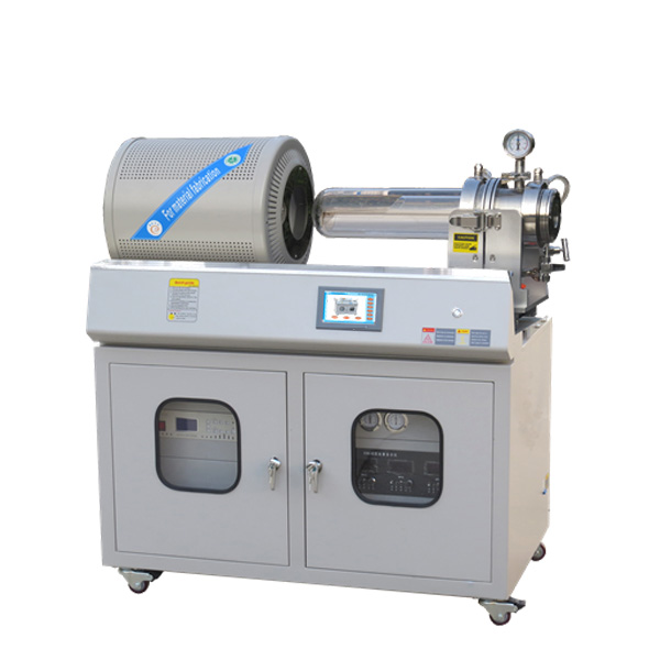
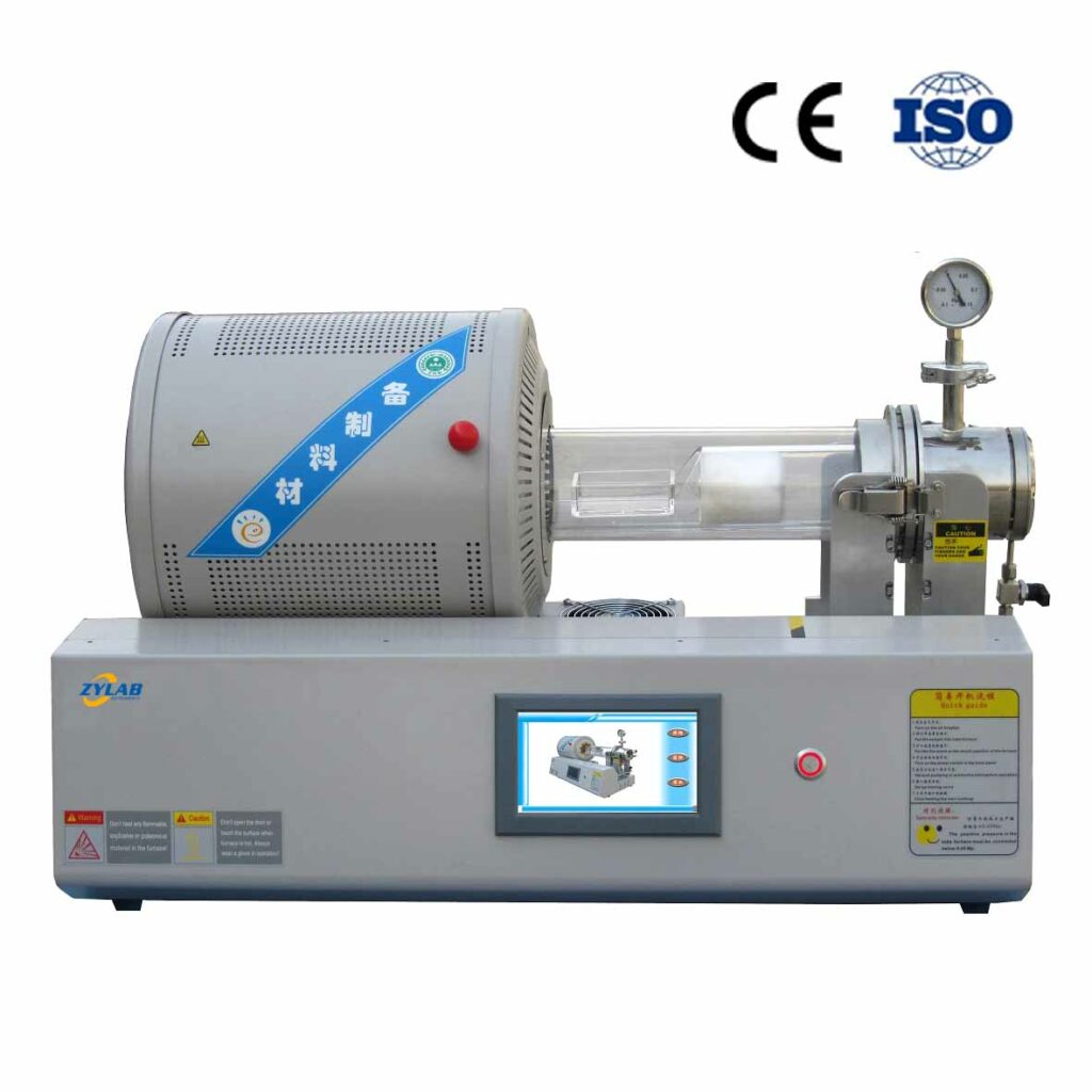
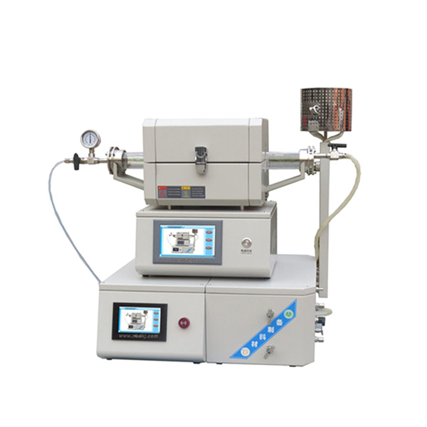
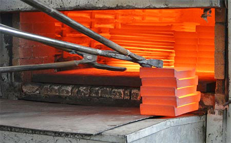
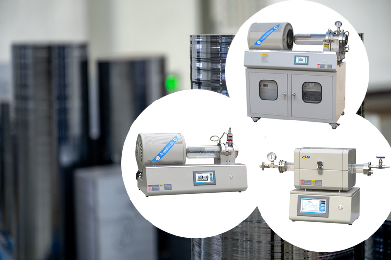
Common Annealing Equipment
Impact of Annealing on Monocrystalline Silicon Performance
Reduction in Crystal Defect Density:
Enhances the material’s crystalline integrity, making it more suitable for producing high-efficiency devices.
Improvement in Carrier Mobility:
Reduces the interference from impurities and defects within the crystal, enhancing the mobility of electrons or holes.
Better Surface Passivation:
For photovoltaic applications, annealing passivates surface defects, reducing surface recombination losses and improving efficiency.
Enhanced Mechanical Properties:
Eliminating residual stress significantly improves the material’s crack resistance and processability.
Applications
Semiconductor Industry:
Used in the production of integrated circuits, transistors, and other devices to enhance material performance and improve production yield.
Photovoltaic Industry:
Boosts the photoelectric conversion efficiency of monocrystalline silicon solar cells, with widespread use in advanced cell technologies such as PERC and HJT.
Sensors and MEMS Devices:
Enhances the reliability and sensitivity of silicon-based sensors and microelectromechanical systems (MEMS).
Through annealing, monocrystalline silicon undergoes significant structural and performance optimization, laying a solid foundation for its applications in high-tech industries.
