Table of Contents
Introduction
In the fast-evolving semiconductor industry, material purity and structural integrity play a pivotal role in determining the performance of electronic devices. One of the most effective methods for achieving high-purity semiconductor materials is hydrogen purge reduction in a controlled furnace environment.
Hydrogen purge reduction furnaces provide an optimal atmosphere to remove oxides and impurities from semiconductor materials, thereby enhancing electrical properties and improving overall device efficiency.
This article explores the working principle, key features, applications, and future trends of hydrogen purge reduction furnaces in semiconductor material synthesis.
How Hydrogen Purge Reduction Works
A hydrogen purge reduction furnace operates by introducing high-purity hydrogen (H₂) gas into a controlled thermal environment, where semiconductor materials undergo reduction reactions. The fundamental process follows these key steps:
- High-Purity Hydrogen Injection – The system introduces ultra-high purity (UHP) hydrogen gas to create a reducing atmosphere.
- Oxide Reduction Reaction – Metal oxides on semiconductor materials react with hydrogen to form water vapor.
- Hydrogen Purging – The continuous flow of hydrogen sweeps away by-products, preventing contamination.
- Temperature Precision Control – Advanced PID controllers maintain precise temperature profiles to optimize material properties.
- Vacuum and Atmosphere Control – Integrated vacuum and gas control systems ensure an ultra-clean environment for processing.
By utilizing this process, unwanted oxides and impurities are efficiently removed, leading to superior material properties essential for semiconductor fabrication.
Key Features of Hydrogen Purge Reduction Furnaces
To meet the stringent requirements of semiconductor manufacturing, modern hydrogen purge reduction furnaces are equipped with advanced features, including:
1. High-Precision Temperature Control
- Multi-zone PID control ensures uniform temperature distribution.
- Customizable heating profiles support various material synthesis requirements.
2. Ultra-Pure Hydrogen Atmosphere
- Integration with gas purification systems to prevent contamination.
- Continuous gas flow monitoring to ensure stable reduction conditions.
3. Vacuum and Inert Gas Compatibility
- Ability to switch between hydrogen and inert gas (argon, nitrogen) for flexible processing.
- Vacuum-assisted gas exchange to minimize oxidation risks.
4. Enhanced Safety Features
- Hydrogen leak detection systems to prevent hazards.
- Explosion-proof chamber design for high-temperature hydrogen environments.
- Automated gas shutoff mechanisms for emergency situations.
5. Scalability and Customization
- Available in small-scale laboratory models to large industrial-scale systems.
- Custom heating zones, automation, and gas mixing options for specialized applications.
ZYLAB’s hydrogen purge reduction furnaces incorporate these cutting-edge technologies, offering superior gas control, multi-stage purification, and intelligent safety features to enhance semiconductor material synthesis.
Applications in Semiconductor Material Synthesis
Hydrogen purge reduction furnaces are extensively used in the synthesis and processing of semiconductor materials, including:
1. SiC (Silicon Carbide) Crystal Growth
- Hydrogen reduction improves crystallinity and removes residual oxygen impurities.
- Essential for power electronics, high-temperature applications, and electric vehicle (EV) components.
2. GaN (Gallium Nitride) Surface Treatment
- Hydrogen etching enhances GaN substrate quality for LED and high-frequency RF devices.
- Reduces surface defects, improving light emission efficiency and electron mobility.
3. Silicon Wafer Annealing and Oxide Removal
- Eliminates native oxide layers from silicon wafers before further processing.
- Enhances dopant activation and junction formation in microchip fabrication.
4. InP (Indium Phosphide) Semiconductor Processing
- Critical for high-speed optoelectronics and telecommunications.
- Hydrogen atmosphere ensures high-purity material production with minimal defect formation.
Conclusion
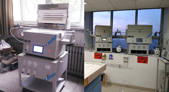
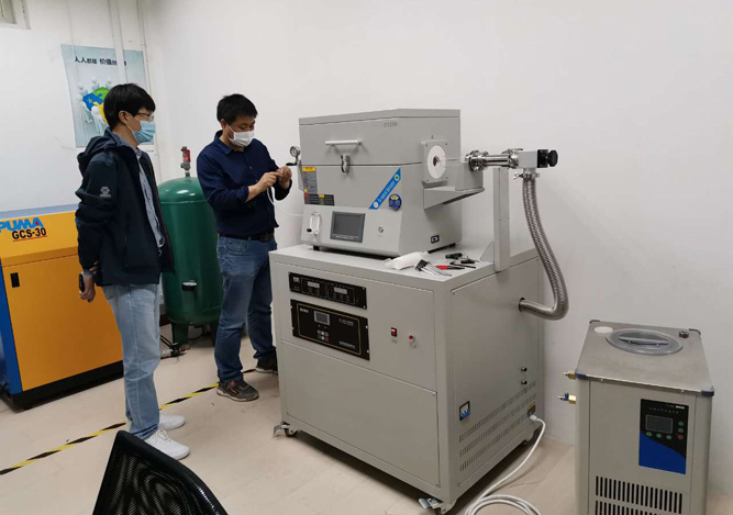
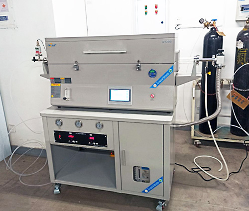
Hydrogen purge reduction furnaces play a critical role in semiconductor material synthesis, offering precise oxide removal, impurity reduction, and improved material quality. Their application in SiC, GaN, InP, and silicon wafer processing is indispensable for producing high-performance electronic devices.
As the semiconductor industry advances, AI-driven optimization, green hydrogen adoption, and larger-scale furnace designs will shape the future of hydrogen-based material processing.
For researchers, manufacturers, and engineers looking to enhance semiconductor fabrication processes, investing in a high-quality hydrogen purge reduction furnace is essential.
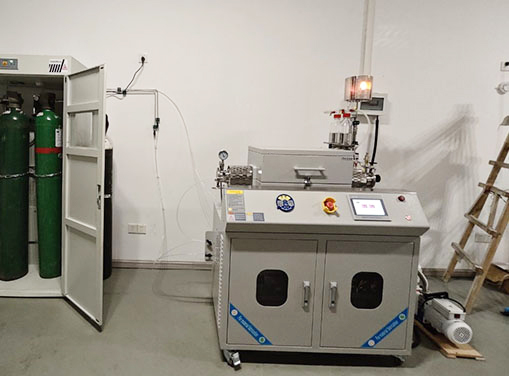
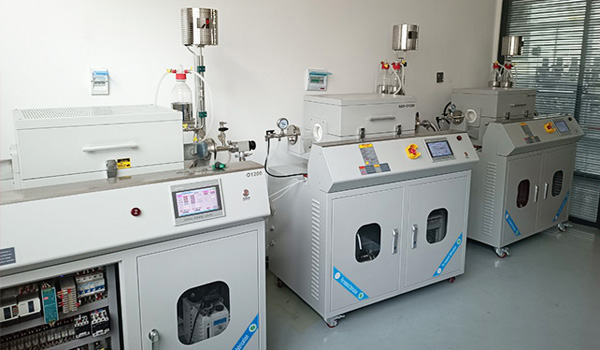
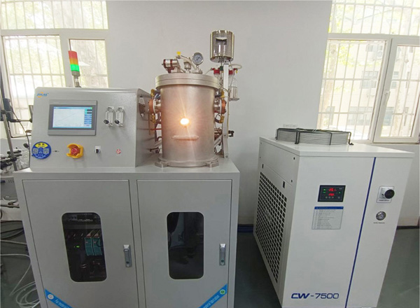
ZYLAB offers cutting-edge hydrogen purge reduction furnace solutions designed for superior performance, safety, and efficiency. Would you like to explore customized solutions for your semiconductor applications? Contact us today to learn more!