Table of Contents
Introduction
Wafer annealing is a critical process in the semiconductor industry that enhances the quality and properties of semiconductor wafers, ensuring their suitability for use in electronic devices. The process involves subjecting semiconductor wafers to high temperatures in a controlled environment to relieve stress, improve crystal structure, and activate dopants.
Achieving precise temperature control, uniform heating, and a clean atmosphere is essential for the success of wafer annealing. This is where large-diameter tube furnaces play a vital role.
In this blog, we will discuss the role of large-diameter tube furnaces in wafer annealing, their key features, technical specifications, and the benefits they offer to the semiconductor industry.
What is Wafer Annealing?
Wafer annealing is a heat treatment process used to modify the properties of semiconductor wafers, which are typically made from materials like silicon or gallium arsenide. The main objectives of annealing include:
- Stress relief: To remove internal stresses created during wafer fabrication.
- Dopant activation: To activate dopants introduced during the doping process.
- Crystal structure improvement: To enhance the crystal structure of the wafer for better electrical performance.
The process requires a furnace capable of providing consistent, high-temperature environments to ensure uniform treatment across the entire wafer.
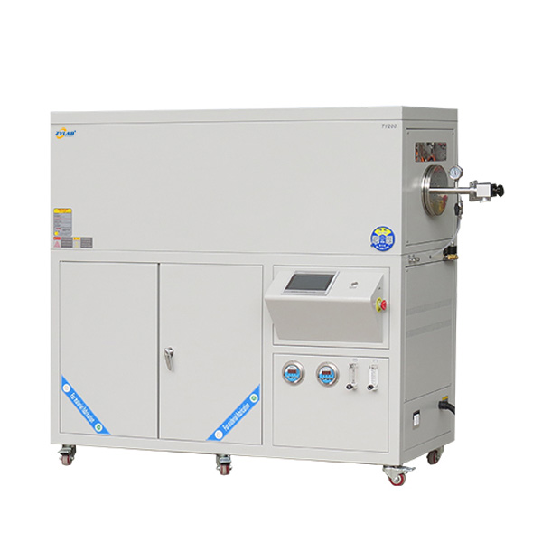
Why Large-Diameter Tube Furnaces are Essential for Wafer Annealing
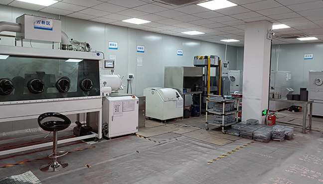
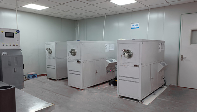
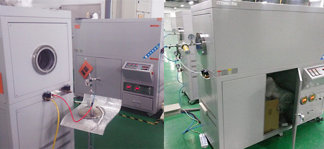
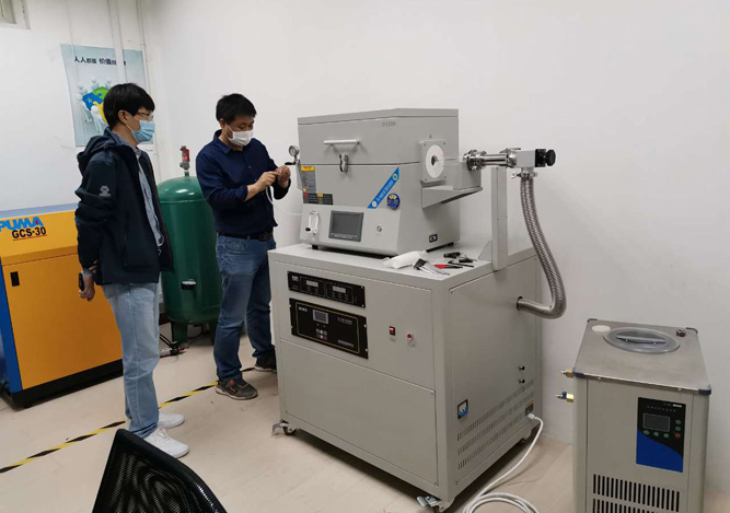
Large-diameter tube furnaces, are engineered to handle high-volume wafer annealing with high precision. These furnaces are designed with several features that make them ideal for semiconductor wafer annealing:
1. Uniform Temperature Distribution
One of the most crucial aspects of wafer annealing is ensuring uniform temperature across the entire wafer surface.
Large-diameter tube furnaces feature a long heating zone and multi-point temperature control, ensuring that the temperature remains consistent throughout the furnace.
This uniformity is vital to avoid hot or cold spots, which can negatively impact the annealing process and result in inconsistent wafer quality.
2. High-Purity Quartz Tube for Clean Processing
The furnace tube is made from high-purity quartz, which is essential for maintaining a contamination-free environment.
In the semiconductor industry, impurities can degrade the quality of wafers, leading to defects in the final product.
The use of high-purity materials ensures that the annealing process is clean, preserving the integrity of the wafers.
3. Precise Temperature Control with Intelligent PID Fuzzy Control
Temperature control is critical in wafer annealing, as even slight fluctuations in temperature can affect the final properties of the wafers.
ZYLAB’s large-diameter tube furnaces are equipped with intelligent PID fuzzy control systems, which ensure that the furnace temperature is precisely regulated.
This level of control helps achieve the desired annealing results, improving the overall efficiency and yield of the semiconductor production process.
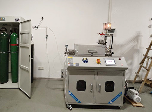
4. Atmosphere and Vacuum Processing Capabilities
Large-diameter tube furnaces offer flexibility in processing under both atmospheric and vacuum conditions.
For wafer annealing, the ability to control the furnace atmosphere—such as introducing nitrogen, argon, or even oxygen—can significantly impact the wafer’s properties.
Additionally, the vacuum capability is particularly useful when processing sensitive materials that must be shielded from contaminants or oxidative environments.
5. Energy Efficiency and Low Power Consumption
ZYLAB’s tube furnaces use high-purity Al2O3 fiber refractory insulation, which significantly reduces power consumption while maintaining excellent thermal insulation.
This energy-efficient design not only lowers operational costs but also ensures that the furnace is sustainable for long-term use in high-volume wafer annealing operations.
Technical Specifications of Large-Diameter Tube Furnaces for Wafer Annealing
ZYLAB’s large-diameter tube furnaces are available in various models, each designed to meet the specific requirements of the semiconductor industry. Here are some key features:
- Tube Diameter: Available in diameters ranging from 152 mm to 215 mm, providing ample space for batch processing and large workpieces such as semiconductor wafers.
- Temperature Range: Capable of reaching up to 1200°C, making them ideal for the high-temperature annealing of semiconductor wafers.
- Heating Rate: With a heating rate of ≤ 20°C/min, the furnace ensures a gradual, controlled ramp-up of temperature, minimizing thermal shock to the wafers.
- Heating Zone Length: Models feature heating zone lengths ranging from 600 mm to 1100 mm, ensuring adequate space for processing multiple wafers simultaneously.
- Power Supply: Options for power supplies ranging from 10KW to 24KW, offering flexibility depending on production scale and furnace size.
Benefits of Using ZYLAB’s Large-Diameter Tube Furnace for Wafer Annealing
- Improved Wafer Quality: Achieve higher-quality wafers with precise dopant activation, stress relief, and crystal structure improvement.
- Increased Production Efficiency: Process large batches of wafers simultaneously, improving throughput and reducing production time.
- Cost-Effective: Lower power consumption and energy-efficient design help reduce operational costs.
- Flexibility: Adaptable to both atmospheric and vacuum processing conditions, making it suitable for a variety of semiconductor applications.
- Long-Term Reliability: Durable design ensures stable performance and longevity in high-volume production environments.
Conclusion
Large-diameter tube furnaces are indispensable in the semiconductor industry, particularly for wafer annealing.
With their ability to provide precise temperature control, uniform heating, and a contamination-free processing environment, these furnaces ensure that semiconductor wafers meet the high standards required for modern electronic devices.
By understanding the advantages of using large-diameter tube furnaces for wafer annealing, semiconductor manufacturers can optimize their production processes, improve wafer quality, and enhance the overall efficiency of their operations.
For more information or technical support, feel free to contact ZYLAB.